Memory chips were originally attached directly to the
system board of a computer. As the need for more memory increased and
the space on the system board started to become scarce, memory chips
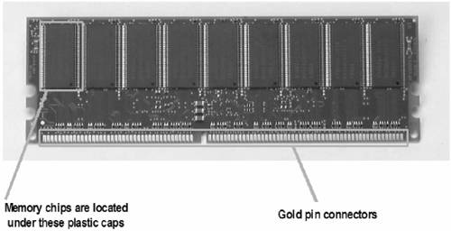
were mounted on cards called memory modules. Figure 1 shows a typical dual inline memory module (DIMM). Notice the parallel rows of memory modules and the gold pin connectors.
The single inline memory module
(SIMM) was one of the first types of memory modules developed. Memory
chips were mounted on one or both sides of a SIMM, but electrical
signals from both sides were routed to the same set of gold pins. SIMMs
could handle only 32 bits of data at a time.
Today's HP ProLiant servers are built to handle
64 bits of data at a time, so SIMMs were eventually replaced by DIMMs.
DIMMs have memory chips on both sides, and each side has separate pins
for a total of 144 pins. Some DIMMs have 168 pins. The extra pins handle
error checking and correcting (ECC) capabilities. (ECC is explained later in this chapter.)
The electrical traces from the memory chips are
routed from the memory chips to gold pins located at the bottom of the
memory module. The pins snap into slots on the system board or a memory
board.
An application-specific integrated circuit (ASIC) known as the memory controller
sits on the system board. The memory controller controls the memory
bus, the pathway between the processor and the memory modules. The
memory bus has two parts: the address bus and the data bus. Figure 2 illustrates how the memory controller utilizes the address bus and data bus.
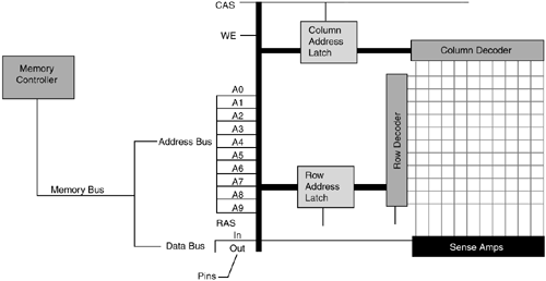
In addition to the address and data pins, a
typical memory module has other pins that it uses to communicate with
the memory controller. The row address strobe (RAS) and column address strobe
(CAS) are pins used to communicate the address of the cell the memory
wants to set. Typically, they carry a high voltage. The memory
controller communicates with the memory chip by changing the voltage of
the RAS and CAS.
The memory controller uses the Write Enable (WE) pin to indicate whether an operation is a read or a write.
To read or write data, the memory controller
sends a row address to the RAS and a column address to the CAS through
the address pins.
For a write operation, data is sent through the Data In pin to the cell at the intersection of the addresses.
For a read operation, a sense amp measures the
charge of the cell at the intersection. If it is charged, the sense amp
indicates a 1 on the Data Out pin. If it is not charged, the sense amp
indicates a 0 on the Data Out pin.
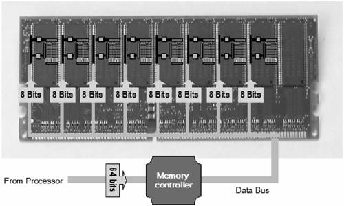
A memory cell can hold 1 bit of data, but a
processor is designed to work with data in bytes. When the processor
needs to store data in memory, it sends 8 bytes of data and an address
through the system bus to the memory controller. The memory controller
breaks each byte of data into 8 bits and uses the address that the
processor sent to determine a row and column address. The memory
controller sends each of the 8 bits to a different memory chip on the
module. All 8 bits will have the same address, just on different chips.
When the processor requests data, the memory
controller sends the same request to each chip, receives the bits of
data, and reassembles them into the requested byte, as illustrated in Figure 3.